

5G and RF ICs — What Engineers Need to Know About Next-Gen Wireless Components

5G and RF ICs — What Engineers Need to Know About Next-Gen Wireless Components
From smartphones to industrial IoT gateways, 5G performance depends on the RF integrated circuits that move signals between the antenna and the digital baseband. This guide walks through 5G RF IC architecture, key components, frequency bands, and the selection parameters engineers use to build reliable wireless hardware.
5G is the latest generation of cellular wireless technology, built to deliver higher data throughput, lower latency, and greater device density than 4G LTE. While much of the conversation around 5G focuses on software, network slicing, and core infrastructure, the physical layer still depends entirely on RF hardware — antennas, filters, amplifiers, switches, and transceivers that condition and route radio signals.
RF integrated circuits (RF ICs) sit at the center of this physical layer. They determine how efficiently a device transmits and receives signals, how much battery or supply power is consumed, how well a design rejects interference, and ultimately whether a product meets the performance targets set by 5G standards. Compared to earlier wireless generations, 5G spans a wider range of frequencies and uses more complex modulation and antenna techniques, which raises the bar for RF component selection, PCB layout, and system-level design.
For telecom engineers, RF engineers, embedded and IoT hardware teams, understanding how RF ICs fit into the 5G signal chain — and what parameters actually matter when choosing them — is essential to building wireless products that perform reliably in the field.
What Are RF ICs?
An RF IC is a semiconductor device designed to generate, amplify, filter, switch, or otherwise process radio-frequency signals. Unlike purely digital ICs, RF ICs work with analog signals at high frequencies, where parasitic effects, impedance matching, and noise behavior become critical design considerations.
In a wireless system, RF ICs form the "RF front-end" — the hardware between the antenna and the digital baseband processor. On the transmit side, the front-end takes a modulated signal from the transceiver, amplifies it to the required power level, and routes it to the antenna. On the receive side, it captures a weak signal from the antenna, filters out unwanted frequencies, and amplifies the signal with minimal added noise before handing it to the transceiver for demodulation. Engineers who are not RF specialists still need a working understanding of this chain, since RF component choices directly affect range, battery life, and regulatory compliance.
RF front-end performance is often the limiting factor in wireless product design — even a well-optimized baseband and antenna cannot compensate for a poorly matched RF signal chain.
5G RF Architecture
A typical 5G RF signal chain includes an antenna, RF filter, RF switch, amplifier stage, and transceiver, connected to the baseband processor. The exact arrangement depends on whether the design uses time-division duplexing or separate transmit/receive paths, but the general flow is consistent across most 5G devices.

Transmit Path
Baseband → Transceiver → Power Amplifier (PA) → RF Filter → RF Switch → Antenna. The transceiver modulates the baseband signal onto an RF carrier, the power amplifier boosts it to the required transmit power, and the filter removes out-of-band emissions before the signal reaches the antenna through the switch.
Receive Path
Antenna → RF Switch → RF Filter → Low Noise Amplifier (LNA) → Transceiver → Baseband. A weak incoming signal is filtered to reject adjacent-band interference, amplified by an LNA with minimal added noise, and then downconverted and demodulated by the transceiver.
Important RF Components in 5G Design

RF Transceivers
The transceiver modulates and demodulates signals between the digital baseband and the analog RF domain. In 5G designs, transceivers must support wider channel bandwidths and, in many cases, multiple frequency bands. Key selection factors include supported frequency range, channel bandwidth, and integration with the baseband processor.
Power Amplifiers (PA)
The PA boosts the outgoing signal to the required transmit power. In 5G, PAs must maintain linearity across wide, high-order modulation signals to avoid distortion, while managing efficiency and thermal output — a balance that becomes harder at higher frequencies and output power levels.
Low Noise Amplifiers (LNA)
The LNA amplifies weak received signals while adding as little noise as possible. Noise figure is the primary selection parameter, since it directly affects receiver sensitivity and the maximum usable range of the wireless link.
RF Switches
RF switches route signals between the transmit and receive paths, or between multiple antennas and frequency bands. In multi-band 5G devices, switch insertion loss and isolation directly affect both transmit efficiency and receive sensitivity.
RF Filters
Filters remove unwanted frequency content from transmit and receive signals, protecting against interference and helping designs meet regulatory emissions limits. As 5G bands sit closer together, filter selectivity becomes increasingly important.
Duplexers
Duplexers allow simultaneous transmit and receive operation on a shared antenna by isolating the two paths. They are common in frequency-division duplex (FDD) implementations and must maintain high isolation to prevent the transmit signal from desensitizing the receiver.
Antenna Matching Components
Passive matching networks — typically inductors and capacitors — tune the impedance between the RF front-end and the antenna. Poor matching increases return loss and reduces both transmit efficiency and receive sensitivity.
RF Front-End Modules (FEM)
FEMs integrate PA, LNA, switch, and filter functions into a single packaged module. They simplify board layout and shorten design cycles, which is one reason they are widely used in space-constrained 5G devices such as smartphones and compact IoT modules.
5G Frequency Bands
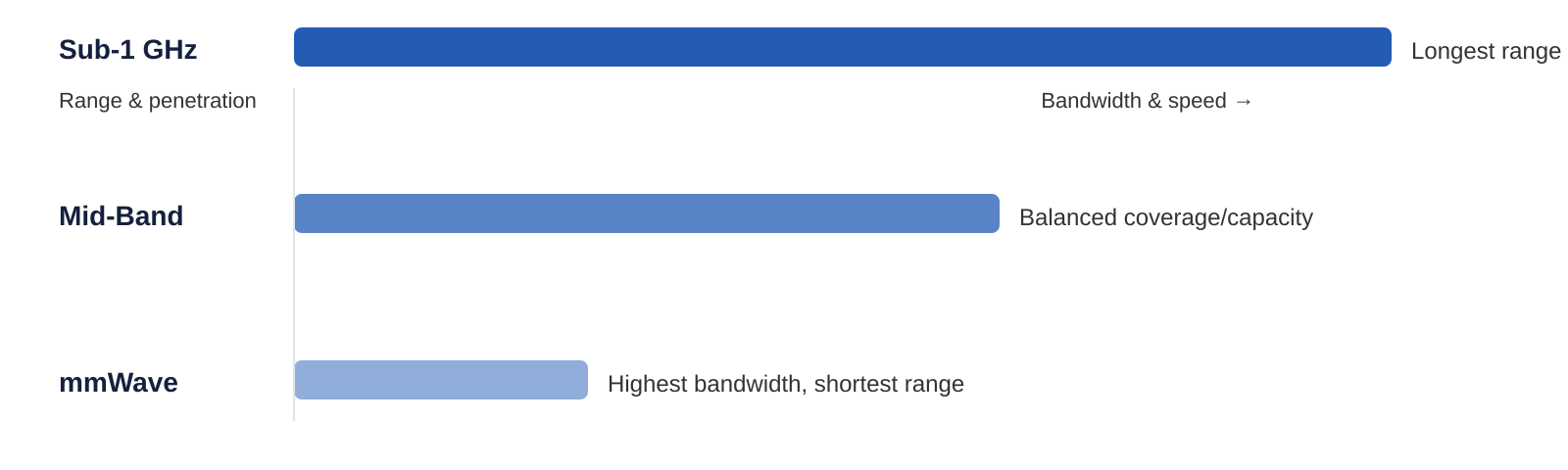
5G operates across three broad frequency ranges, and the choice of band significantly influences RF component selection and overall system design.
- Sub-1 GHz: Offers the longest propagation range and best building penetration, making it useful for wide-area coverage, at the cost of lower available bandwidth.
- Mid-band (roughly 1–6 GHz): Balances coverage and capacity, and is widely used for general 5G deployment.
- mmWave (above 24 GHz): Provides very high bandwidth and data rates over short distances, but signals attenuate quickly and are more sensitive to obstructions.
Higher frequencies generally mean shorter range, greater sensitivity to path loss, more demanding antenna design, and tighter RF component tolerances. mmWave designs in particular require careful attention to insertion loss in traces and connectors, along with thermal management, since RF losses increase with frequency and component density.
Key RF IC Selection Parameters
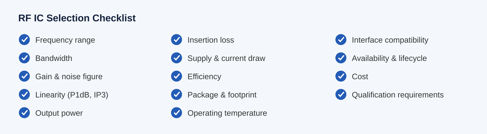
When evaluating RF ICs for a 5G design, engineers typically work through the following checklist:
- Frequency range: The band(s) the component must support.
- Bandwidth: Channel width the component can process.
- Gain: Amplification provided, relevant for PAs and LNAs.
- Noise Figure: Added noise, critical for receive-side sensitivity.
- Output power: Maximum transmit power capability.
- Linearity, P1dB and IP3: Measures of how well a component avoids signal distortion near its operating limits.
- Insertion loss: Signal loss through passive components such as filters and switches.
- Supply voltage and current consumption: Power budget impact, especially for battery-powered devices.
- Efficiency: Ratio of RF output power to DC input power, particularly for PAs.
- Package: Footprint and mounting requirements on the PCB.
- Operating temperature: Rated range for the target application environment.
- Interface: Control and data interface compatibility with the rest of the system.
- Availability and lifecycle: Manufacturer supply status and expected production life.
- Cost: Unit price relative to project budget and volume.
- Qualification requirements: Industry or regulatory certifications the component must meet.
RF Component Consideration Table
| Parameter | RF Component Consideration | Why It Matters |
|---|---|---|
| Frequency | Must match target 5G band(s) | Determines range, penetration and antenna design |
| Bandwidth | Wider channels supported for 5G NR | Impacts achievable data throughput |
| Gain | Sufficient for link budget without saturation | Affects signal strength and distortion risk |
| Noise Figure | Low noise figure on receive chain | Directly affects receiver sensitivity and range |
| Output Power | Meets regulatory and link requirements | Determines coverage and compliance |
| Linearity | Maintains signal integrity near peak output | Prevents distortion in complex modulation schemes |
| Power Consumption | Optimized for device power budget | Critical for battery-powered and IoT devices |
| Package | Compact, PCB-compatible footprint | Impacts board layout and assembly |
| Operating Temperature | Rated for target deployment environment | Ensures reliability in field conditions |
| Availability | Confirmed supply from authorized sources | Reduces project and production delays |
| Lifecycle | Active status with defined roadmap | Lowers risk of obsolescence and BOM disruption |
5G vs 4G RF Component Requirements
5G generally requires wider channel bandwidths, support for a broader set of frequency bands, and more advanced antenna configurations than 4G LTE. This translates into RF front-ends with more components, tighter linearity and noise requirements, and greater attention to power efficiency, since 5G devices often need to support multiple bands and higher data rates within similar power and thermal budgets. RF complexity also increases with the addition of mmWave support, carrier aggregation, and more sophisticated switching between bands, all of which place additional demands on filters, switches, and amplifier design compared to typical 4G implementations.
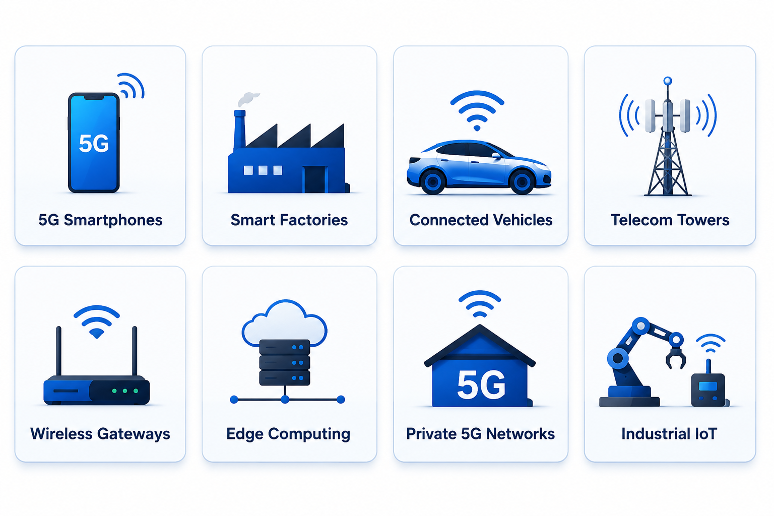
Practical Applications of 5G RF ICs
5G RF components appear across a wide range of product categories:
- 5G smartphones: Use multi-band front-end modules integrating PAs, LNAs, switches, and filters in a compact footprint.
- Industrial IoT devices: Rely on RF transceivers and front-end components tuned for reliability in electrically noisy environments.
- Private 5G networks: Depend on base station RF hardware with high linearity and precise filtering for dense deployments.
- Smart factories: Use RF modules for low-latency machine communication and sensor connectivity.
- Connected vehicles: Require RF front-ends rated for wide temperature ranges and automotive-grade qualification.
- Wireless gateways: Combine multiple RF transceivers and antenna paths to bridge different network types.
- Telecom infrastructure: Uses high-power PAs, precision filters, and duplexers to serve wide-area coverage.
- Edge computing devices: Integrate RF ICs alongside processing hardware for on-site data handling.
Engineering Design Considerations
Selecting the right RF ICs is only part of a successful 5G design. Board-level and system-level factors play an equally important role:
- PCB layout: RF traces require controlled impedance and careful routing to minimize loss and reflections.
- Impedance matching: Mismatches between components and the antenna reduce efficiency and increase return loss.
- Grounding: A solid, low-inductance ground plane is essential for RF stability.
- Thermal management: PAs and other active components can generate significant heat that must be managed for reliability.
- EMI/EMC: RF designs must be shielded and filtered to avoid interference with other subsystems.
- Signal integrity: High-frequency signals are sensitive to trace length, via placement, and layer transitions.
- Antenna integration: Placement and matching between the antenna and RF front-end affect overall system performance.
- Component placement: Proximity between RF stages minimizes loss and unwanted coupling.
- Power integrity: Stable, low-noise power delivery is required for consistent RF performance.
Validate RF component footprints and matching networks early in the layout process — late-stage RF changes are far more costly than digital or power layout revisions.
Component Availability & Lifecycle
Engineering performance is only one side of RF component selection. Long-term production success also depends on supply-chain factors: manufacturer lifecycle status, lead times, and the availability of second sources or verified alternates. RF ICs with limited availability or an approaching end-of-life status introduce BOM risk that can disrupt production well after a design has been finalized.
Engineers should evaluate component selection alongside sourcing considerations from the earliest design stages — checking manufacturer roadmaps, identifying pin-compatible alternates where possible, and working with distribution partners who can flag obsolescence risk before it affects production continuity.
Build BOM resilience by identifying at least one qualified alternate for critical RF components before committing to a production run.
How Indus Technologies Supports Wireless & RF Component Requirements
Indus Technologies supplies electronic components and semiconductor components to engineering and product teams working on wireless and RF designs. For teams building 5G-capable hardware, this includes support for sourcing RF and communication ICs, along with component sourcing and BOM support for project-level procurement.
Beyond component supply, Indus Technologies offers design and software services to help teams move from concept to production. Engineers evaluating RF and wireless components for a new design can reach out through the contact page for procurement or sourcing support tailored to their project.
Looking for the Right RF & Wireless Components?
Explore electronic components and sourcing solutions from Indus Technologies.
Explore ComponentsFrequently Asked Questions
RF ICs are semiconductor components designed to generate, amplify, filter, or switch radio-frequency signals as part of a wireless system's transmit and receive chains.
5G devices must handle wider bandwidths, more frequency bands, and stricter linearity and noise requirements than earlier generations, all of which depend directly on RF IC performance.
The RF front-end is the set of components between the antenna and the transceiver, typically including filters, switches, amplifiers, and duplexers, that condition signals for transmission and reception.
Selection is based on parameters such as frequency range, bandwidth, gain, noise figure, linearity, power consumption, package, and long-term availability, matched to the target application's requirements.
Frequency range, noise figure, linearity (P1dB and IP3), output power, insertion loss, power consumption, operating temperature, package footprint, and manufacturer lifecycle status are all key checks before finalizing an RF IC.
Conclusion
RF ICs remain the foundation of every 5G wireless system, from smartphones to industrial gateways and telecom infrastructure. As 5G hardware grows more complex — spanning wider frequency bands, tighter linearity requirements, and denser RF front-ends — engineers need to weigh performance parameters like noise figure, gain, and power consumption alongside practical factors such as PCB layout, thermal management, and component availability.
Getting RF component selection right early in the design cycle — and maintaining a resilient BOM through the product's lifecycle — helps engineering and product teams bring reliable 5G hardware to market with fewer surprises. Indus Technologies supports this process with sourcing for electronic and semiconductor components, including RF and wireless ICs, for teams building next-generation wireless products.
-

-

November 27, 2025
Connecting the Dots: How Electronic Components Work Together in Devices -

November 27, 2025
How reliable is your electronics components supplier